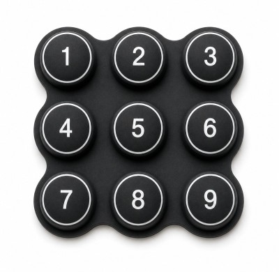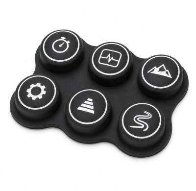
Silicone Keypad for Heavy Equipment Control Panels: PCB Alignment Issues Before Tooling
Silicone Keypad for Heavy Equipment Control Panels: PCB Alignment Issues Before Tooling
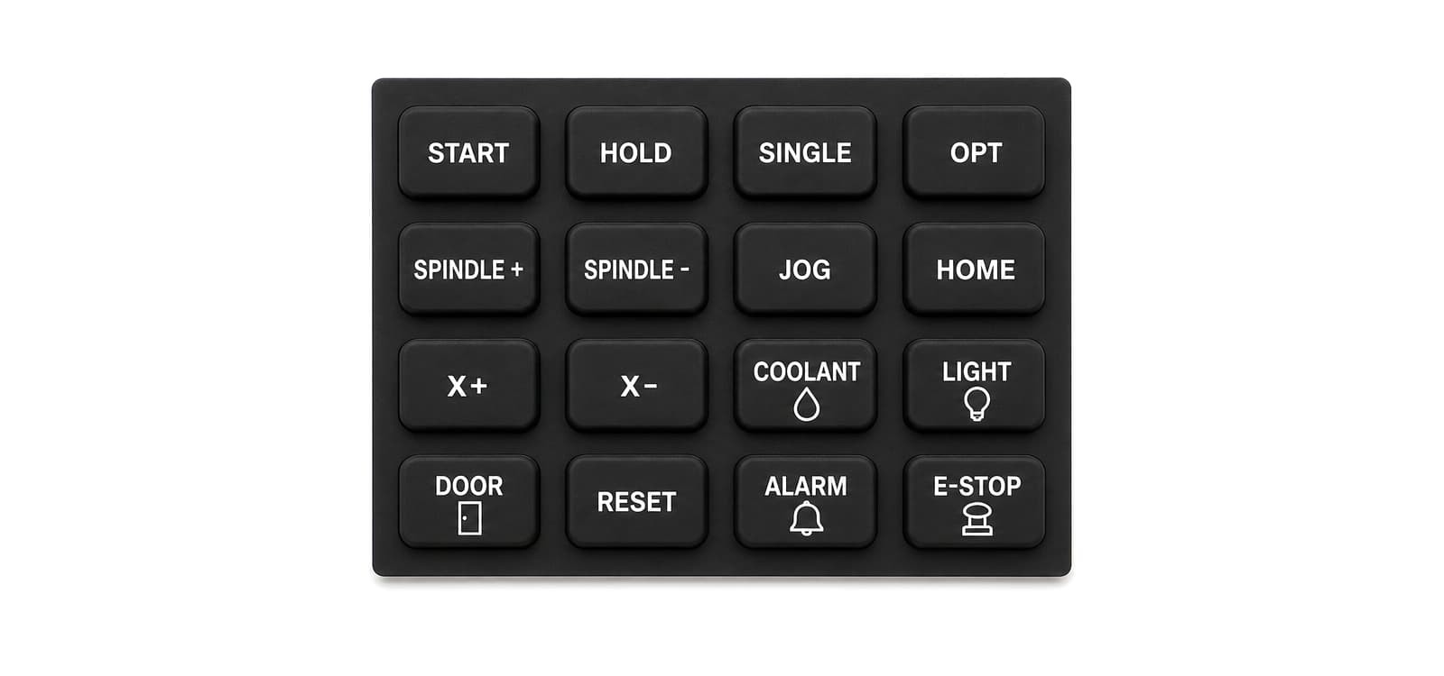
The first time a heavy equipment panel misbehaves, the fault rarely looks like a keypad problem. A START button feels crisp on one machine and mushy on the next, and a panel that behaves all morning drops inputs after hours on a dusty site. Engineers suspect the switch; more often the trouble sits at the interface between a moulded Silicone Keypad for Heavy Equipment and the board underneath it.
A keypad is a mechanical system before it is an electrical one, and the decisive choices are pill against pad, keypad edge against housing, travel against switching point. Get those wrong and the correction arrives after tooling, not before it.
Introduction - Why PCB Alignment Matters in Heavy Equipment Silicone Keypad Design
Alignment is a stack-up question. Silicone keypad geometry, PCB contacts, conductive pills, the support structure, and the force and travel budget connecting them: five contributors, each with a tolerance band, and the button only works when all five land inside a window narrower than any one of them.
Where the misalignment is discovered decides the cost: a redline at the drawing stage, electrodes and a schedule slip after the mould is cut, and an argument after assembly, when the housing is already in production. This discussion stays inside the keypad-to-PCB interface.
How a Silicone Keypad Interfaces with a Heavy Equipment Control Panel
The interface is a compression joint: the keypad is squeezed between housing and board, and every electrical event happens inside that squeeze.
Basic Components of the Interface
A typical heavy equipment silicone keypad is one moulded silicone body; everything else is moulded into it, pressed against it, or bolted around it.
- Silicone keypad body: the moulded part carrying every button, the perimeter skirt and the clamped frame.
- Buttons and flexible webs: each cap sits on a web that deforms under the press and returns it, setting force and travel.
- Conductive carbon pills: carbon-loaded pads moulded under each button, or a printed layer, forming the moving half of the contact.
- PCB contact pads: interdigitated fingers or carbon-printed pads, spaced to match the button pattern, forming the stationary half.
- Housing support: the rigid structure that compresses the keypad and fixes how much squeeze the webs see.
- Locating features: pins, holes and slots that stop the keypad drifting sideways relative to the pad pattern.
Only two of those six are usually drawn to the same tolerance philosophy: the board comes from a shop working to fine positional tolerances, the housing from a moulder working to coarser ones.
Why Heavy Equipment Applications Require More Careful Alignment
Vibration comes first. A cab-side panel lives with continuous low-amplitude motion, which the machine builder characterises using the framework of ISO 20816-1:2016. The keypad does not need to shake visibly to suffer: a fraction of a millimetre of relative movement, repeated thousands of times a shift, is enough to work a marginal contact toward intermittent behaviour.
Repeated operation and contamination follow. The press count is higher than a design meeting usually assumes, and dust, cutting fluid and oil change the friction between keypad edge and housing wall and collect in any gap wide enough to admit them. Whatever encloses the panel is classified under the protection scheme of IEC 60529, and the keypad aperture is part of that enclosure.
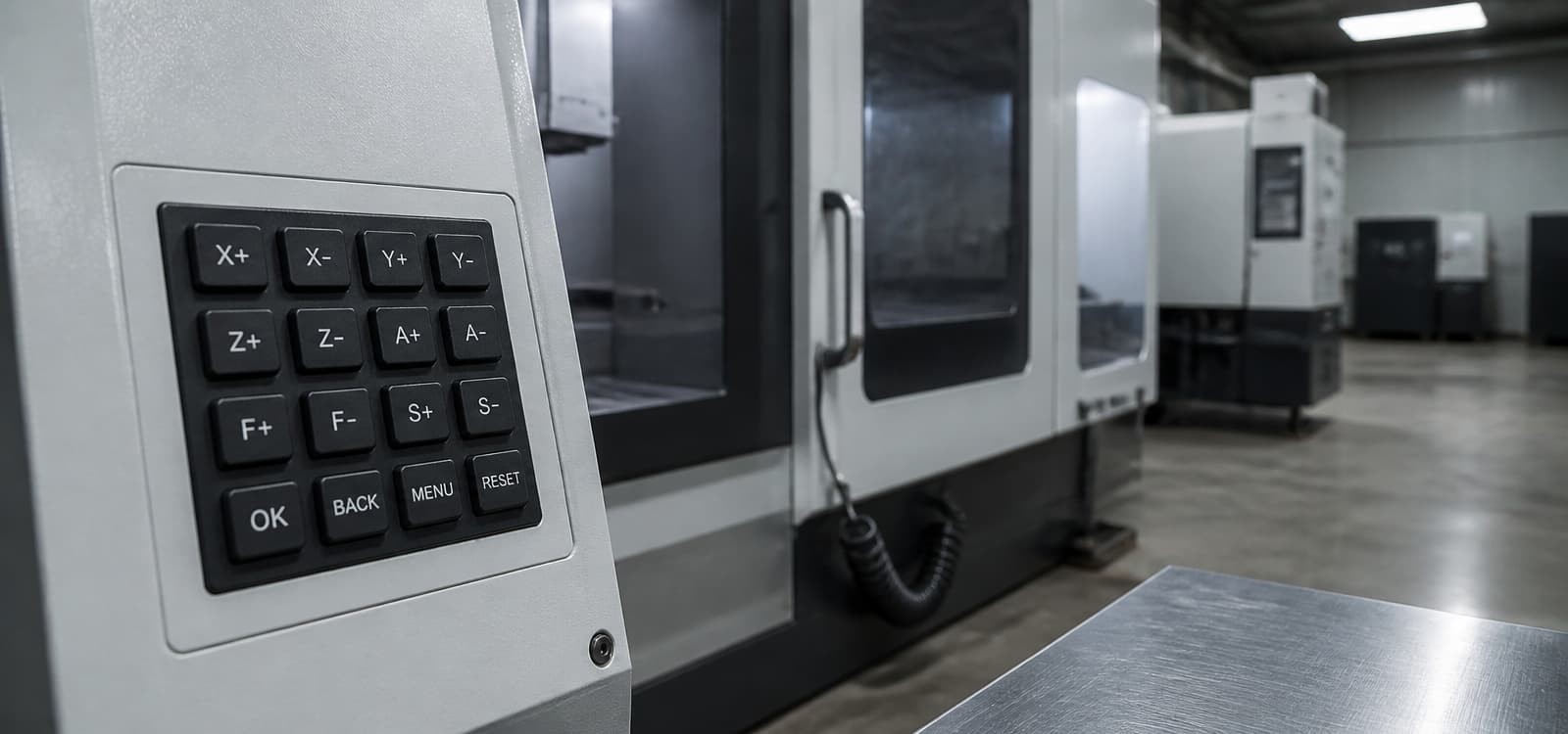
Gloved operation dulls the sensation of a weak button, and a button 300 mm from the locating pin inherits every dimensional error between that pin and itself.
Common PCB Alignment Problems Before Silicone Keypad Tooling
Four faults account for most of the rework that arrives after a heavy equipment panel keypad has been tooled. All four are visible on paper.
Conductive Pill Does Not Match the PCB Contact Pad
The pill must land on the pad pattern with enough overlap to close the circuit in the worst case of off-centre travel. When button spacing came from an old board revision, or the housing lets the sheet shift, the pill bridges the pad fingers unevenly: one edge touches first, current crowds through a smaller area, and contact resistance climbs.
The symptom is not a dead button. It is a button that works on the bench and needs a second press a few months later, the pattern documented in this comparison of carbon pills that fail to match PCB pads.
Keypad Dimensions Do Not Match the PCB Layout
Overall dimensions and button pitch are the figures most often copied from a summary drawing instead of the board itself, and overall length can be right while the pitch between clusters is wrong. Board revisions make it worse: if the keypad drawing references revision B while the line still builds revision A, the outer buttons are misaligned before assembly. A moulded part cannot hold a fine pitch across a 250 mm span either, so review both drawings together, as a pair, against one coordinate system.
Button Travel Does Not Match the Electrical Contact Position
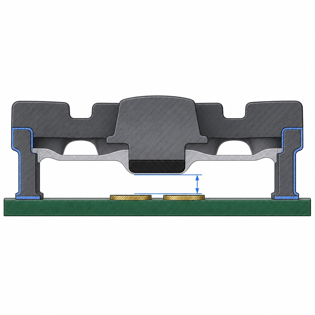
Travel and the switching point are two different events, and designs fail when nobody states where the second one happens. Travel is how far the cap moves from rest to the bottom of its stroke; the switching point is where the pill touches the pad and closes the circuit. In a sound design it sits comfortably before the bottom of travel, so the press is definite and the pill still has follow-through.
Web geometry sets how far the button can move, pill position decides when it reaches the board, and pad height with any solder mask step sets the real contact plane. If the switch point falls too early, a light brush triggers the button; if too late, the operator bottoms the button out and contact force varies between buttons.
Housing and Locating Features Are Missing
If the housing does not positively position the keypad, the moulding is positioned by whatever is left: friction, the perimeter skirt, or the first screw tightened. Pins, locating holes, retaining features and local supports remove that freedom, which matters most on long and curved panels where one pin leaves the far end free to lift. Assembly-stage shift is examined further in this note on button alignment problems during PCB assembly.
| Symptom reported | Interface layer to check first |
|---|---|
| Some buttons need a firm press, others respond lightly | Switch point versus travel across buttons |
| Works new, degrades after months | Pill overlap and web compression set |
| One row responds poorly, others are fine | Pitch error accumulating across the panel |
| Resistance drifts between batches | Mould shrinkage against pad position |
PCB Information Engineers Should Prepare Before Tool Development
A mould cannot be corrected by wishful measurement, so the data handed to the tool designer decides how much alignment work gets solved on paper.
Essential PCB Drawings and Data
Start with the board, in the coordinate system the board shop uses.
- PCB outline with the panel cut-out relationship, so keypad edge and aperture share one origin.
- Button centre coordinates in X and Y for every button, not only the outer ones.
- Contact pad dimensions, and whether the pad is copper, gold-plated or carbon-printed.
- Pad spacing and orientation: a pad rotated 90 degrees changes the overlap available to the pill.
- PCB thickness and finish, since solder mask over a pad pattern raises a step in the contact plane.
- Mounting hole locations, which fix how the board sits relative to the housing.
- Tall components and connectors near buttons that could interfere with the skirt or frame.
Mechanical Housing Information
The housing sets the compression budget, and it is the part most often described in prose instead of millimetres.
- Available installation depth from panel face to board surface, including the panel's own tolerance.
- Closed compression height, as a range rather than a nominal figure.
- Housing material, because moulded plastic, cast metal and sheet metal hold flatness differently.
- Retaining structure: screw bosses, snap fits, clamps or a bezel, plus the tightening order.
- Surface curvature, since a flat keypad in a curved housing develops a different gap at the ends.
- Screw boss positions and heights, because boss variation tilts the assembly and moves outer buttons first.
Electrical Contact Requirements
These figures depend on the board and the application rather than on a general rule.
- Conductive pill size: moulded diameter and height, chosen to overlap the pad with margin for positional error.
- Contact resistance expectation for the assembled panel, not for a bare pill on a bench.
- Contact pad finish: copper, gold and carbon behave differently under repeated contact and oil films.
- Required actuation force as a range an operator in gloves can feel, stated per button group.
- Switching behaviour: momentary, maintained or dual-level, which sets how much travel remains after contact.
No universal pill size or resistance figure applies across panels, and a supplier quoting one without seeing the board is guessing. Hardness sits in the same category: ASTM D2240 covers durometer measurement, but the useful figure depends on the web geometry carrying it.
Tolerance Considerations for Heavy Equipment Silicone Keypad Design
Alignment survives on arithmetic, and four tolerance sources feed the same interface without sharing a reference. Mould dimensions carry the cavity's machining tolerance. Shrinkage varies with wall thickness, cure conditions and flow direction, which is one reason batch drift shows up on long runs. Board tolerances are tight in position but not zero, and housing tolerance is usually the loosest and arrives last, after the keypad is made. When those effects combine, failures that look electrical turn out to be dimensional, as in this account of keypad failures in high-vibration environments.
Why Tolerance Stacking Can Cause Alignment Problems
A stack-up only means something against a common reference. Three planes usually serve as datums: the PCB top surface where the pads sit, the housing locating bore that positions the keypad, and the shoulder the keypad frame seats against. Three moulded parts sit in that chain - the silicone keypad, the housing front cover and often a retainer or bezel. Measure from the wrong plane and the stack looks healthy while the button does not work.
One illustrative case, not a rule. On a 250 mm panel with a button 120 mm from the locating pin, suppose shrinkage and cavity variation pull the moulding 0.4 percent across that span, roughly 0.5 mm. Add 0.1 mm of board-level pad placement, 0.15 mm of locating bore clearance and 0.2 mm of assembly shift. Worst case, the pill centre lands near 1 mm from where the pad was drawn - close to a third of the overlap gone on a 3.5 mm pad pattern before the first shift of work, and not in the same direction on every unit.
So measure rather than estimate: press the keypad into the housing, close the assembly, and record pill position on the outermost buttons, not just the centre one.
Designing Locating Features to Reduce Assembly Variation
Locating features cost less than tolerance.
- Two locating holes matched to housing posts, separated as widely as geometry allows so the part cannot rotate.
- Positioning posts that contact the keypad frame, never the webs, so locating load misses the moving parts.
- A stiffer perimeter or internal rib that holds button pitch through moulding and curing.
- Defined ribs or pads on the housing that set exactly where the keypad is squeezed, and how much.
- Directional clearance: loose where the panel expands, tighter in the axis deciding pill-to-pad position.
How Silicone Keypad Geometry Affects PCB Contact Reliability
Once the drawings agree, geometry decides whether the contact stays reliable or only tests well on the bench. Pill, web and button height are what a moulding supplier controls directly, and they are where a review of the silicone rubber keypad build details starts.
Conductive Pill Diameter and Position
The pill is a moving contact, so its working area is the overlap with the pad at closure, not its own diameter. A larger pill buys tolerance margin but spreads the same web force over more area and lowers contact pressure; a smaller one sharpens the switching feel with less room for positional error. Position matters as much as size: a pill moulded off the button axis still has to sit on the pad centre once the keypad is assembled into the housing, so the moulded position is checked against the housing datum.
Silicone Web Thickness and Button Travel
The web is the spring and the tolerance absorber at once. Thickness and unsupported span set actuation force, return speed and how much travel remains after contact. A thin web gives a light press and quick return with little reserve force; a thick web gives a definite feel, then demands more travel and more finger load over a long shift.
Button Height and Surface Geometry
Button height is the gap between the housing face and the board, minus the compression the assembly applies, so it is not a keypad decision taken alone. Too tall and the housing pre-loads the webs, so buttons feel stiff and the silicone takes a set early; too short and the pill barely reaches the pad. The surface above it, whether flat or a defined thumb pad, changes the contact patch of a gloved finger and belongs in the panel layout discussion.
Common Mistakes When Developing a Heavy Equipment Silicone Keypad
Seven errors repeat across projects.
- Starting mould development without a finalised PCB drawing. The tool is cut to an interim revision. Freeze the pad layout first.
- Using overall dimensions without button coordinates. Outer buttons line up while the middle drifts. Require per-button coordinates.
- Ignoring housing locating structures. Friction and screw order position the keypad, so a few units per batch shift. Specify pins or holes.
- Changing the PCB layout after the mould is complete. Contact overlap falls away on one side. Treat any board change as a formal change.
- Leaving actuation force undefined. Buttons feel different across the panel. State a range per button group.
- Overlooking assembly compression. Webs sit pre-loaded and take a set; ISO 815-1:2019 defines compression set as the deformation remaining after compression is released. Define the closed height.
- Treating every button as identical. A jog button pressed thousands of times a shift has different duty. Group buttons by function.
Recommended Design Review Process Before Mold Manufacturing
- Collect PCB and housing drawings - board, housing and panel cut-out sharing one origin.
- Confirm button locations and contacts by overlaying the pad pattern on the button centres and checking every button.
- Review keypad geometry: pill size and position, web thickness and span, button height, frame stiffness.
- Check mechanical tolerances by building the stack from named datums and finding the dominant contributor.
- Confirm material and contact requirements: hardness, finish, pill or printed layer, wear and oil exposure.
- Review prototype or 3D data: a prototype pressed into the actual housing finds interference faster than discussion.
- Approve tooling drawings, signing off keypad drawing and electrode layout together and recording the revision.
Outside review helps most at steps two and four, where the board and the rubber meet: technical support for keypad and panel design.
What a Custom Silicone Keypad Manufacturer Should Confirm
- Keypad dimensions: overall size and datum, matched to the housing aperture rather than the panel outline.
- Button spacing: per-button coordinates confirmed against the current board revision.
- Conductive contact requirements: pill diameter and position, or printed layer, with required pad overlap.
- Material hardness, selected for the web geometry and the feel the panel needs.
- Tactile force: target range per button group, with the test method and deflection used.
- Surface printing: legend content, colour, placement and wear expectation under gloves and oil.
- Backlighting: light guides, translucent legends, and the light path against the pill side.
- Assembly method: how the keypad is retained, in what order, and to what closed height.
Conclusion
PCB alignment in a Silicone Keypad for Heavy Equipment is settled at the interface, not by the machine: pill against pad, keypad against housing, travel against switching point. Each relationship is on paper before the mould exists, which is where the work is inexpensive.
Heavy equipment raises the stakes: vibration, repeated operation, dust and gloved use consume margin a small panel would never notice, and on a wide panel the far buttons inherit every dimensional step between them and the locating pin.
FromRubber, the brand of Dongguan Bohao Electronic Technology Co., Ltd., has manufactured custom silicone and plastic parts since 2010 and works from customer drawings, samples or sketches, the stage at which these questions are least disruptive to answer.
FAQ
Why does PCB alignment matter in a silicone keypad?
The electrical contact exists only where the conductive pill overlaps the PCB pad. Alignment decides how much of that overlap survives shrinkage, board tolerance and assembly shift.
What information is needed before developing a custom silicone keypad mold?
Board outline, per-button centre coordinates, pad dimensions and spacing, board thickness and finish, and mounting hole positions. From the mechanical side: installation depth, closed compression height, housing material, retaining structure and screw boss locations.
Can a silicone keypad be redesigned to match an existing PCB?
Yes, and it is the usual starting point when a panel already exists. Keypad geometry, pill placement and web design are adjusted to the board rather than the other way round.
How do conductive carbon pills work with PCB contacts?
The carbon-loaded pill acts as a moving bridge across a pad pattern, usually interdigitated fingers. Depressing the web lands the pill on the pattern and closes the circuit; the returning button opens it again.
What causes intermittent contact in heavy equipment silicone keypads?
The common causes are pill offset from the pad centre, insufficient closing force from the web, and assembly shift allowed by weak locating features. Machine vibration then turns a marginal contact into an unreliable one.
Sources and standards referenced
- ISO 20816-1:2016 Mechanical vibration - Measurement and evaluation of machine vibration - Part 1. https://www.iso.org/standard/63180.html
- ASTM D2240 Standard Test Method for Rubber Property - Durometer Hardness. https://store.astm.org/d2240-15r21.html
- ISO 815-1:2019 Rubber, vulcanized or thermoplastic - Determination of compression set. https://www.iso.org/standard/74943.html
- IEC 60529 Degrees of protection provided by enclosures (IP Code). https://webstore.iec.ch/en/publication/2452