Uneven Carbon Pill Distribution in Industrial Remote Silicone Keypads: How Molding Process Affects Contact Resistance Consistency
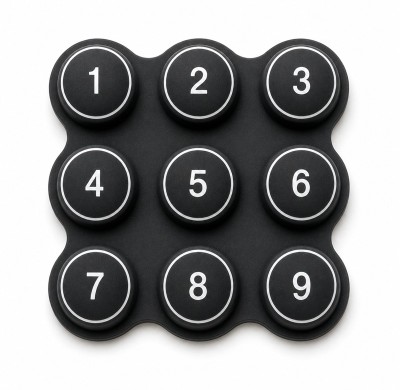
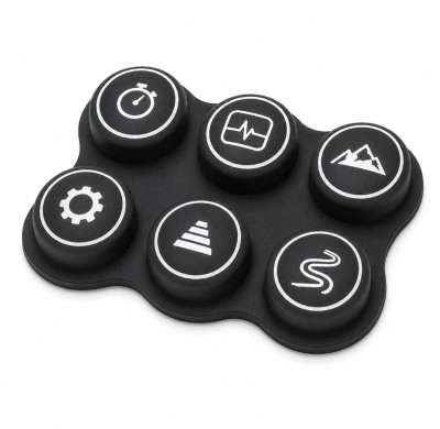
Two buttons. Same drawing. Same PCB. The one on the left measures 90 ohms, the one on the right measures nearly 400. Both pass a simple continuity check, so both get shipped, and three months later the field returns start arriving with a complaint that says "the right-hand keys feel dead". This is the most common conductive-silicone problem we get asked about, and in most cases the mould is blamed long before anyone has measured the pills.
Why Contact Resistance Can Vary Between Silicone Keypad Buttons
What the Conductive Carbon Pill Does
A conductive carbon pill is not a switch in the electromechanical sense. It is a small disc of carbon-loaded silicone, co-moulded into the underside of the key, that bridges a pair of interlaced PCB pads when the key is pressed. The resistance you measure is therefore the sum of several things happening at once: how well the carbon-loaded silicone conducts through its own thickness, how much real contact area is actually touching copper, and how much of the copper is covered by oxide, flux residue or solder mask that should not be there.
That matters because the first two terms are set by the keypad supplier, and the third is set by the assembly line. When a returned part reads 400 ohms, the honest answer is usually "we do not know yet which of the three it is" until the pill is inspected against the PCB it was paired with.
Why Identical Keypad Designs May Still Produce Different Resistance
Two cavities in the same tool can produce keys that measure differently even though the drawing is identical. The reason sits in a handful of variables that never appear on the drawing: the actual pill diameter after cure shrinkage, the finished pill thickness, the parallel flatness of the contact face, the local packing of carbon black through the pill cross-section, and the compression the key sees when the assembly is closed.
Conductive silicone is a percolation system. Carbon black does not carry current uniformly through the material, it carries current through a network of touching and near-touching particles. That network is highly sensitive to how the compound flows. A pill that was compressed slightly more during moulding can end up with a marginally denser particle network in one region and a leaner one next to it, and the resulting resistance difference across a 4 mm disc can easily be a factor of two.
Resistance Variation vs. Complete Conductive Failure
It helps to separate four conditions that get described with the same words in production meetings. Normal tolerance is a part-to-part spread that stays inside a defined band. Position-to-position variation is a spread between keys within one keypad. Intermittent conductivity is a reading that changes when the key is pressed at a different angle or force. Open-circuit failure is a pill that never conducts, which is usually a material or assembly defect rather than a distribution problem.
Only the middle two are genuinely the subject of this article. An open circuit is a different investigation.
Reading the pill before blaming the circuit
Before any measurement is taken, photograph the pill face and the PCB pads together at the same magnification. A pill that has shifted off the pad pair by 0.2 mm looks perfectly normal from the top of the key. This is why the first diagnostic step is always visual, and why the second step is measuring at several positions rather than at one convenient button.
How Uneven Carbon Pill Distribution Develops During Molding
Conductive Material Positioning Before Compression
In compression moulding, the conductive compound is placed in the cavity as a pre-formed pellet or a weighed slug before the mould closes. Its position relative to the intended pill centre is the first place tolerance enters the process. If the slug sits slightly off-centre, the closing mould pushes material laterally, and the resulting pill can be egg-shaped rather than round, with a thinner wall on one side.
Compression Flow and Material Movement
Once the mould closes, the compound has to flow into the pill cavity, the key wall and the connecting web. Those three regions have very different volumes, so the flow front does not arrive everywhere at the same time. Where the flow front meets a wall, the material orientation changes, and on a carbon-filled compound that orientation is not entirely erased by cure. Local thickness differences of a few hundredths of a millimetre on the pill face translate directly into contact-area differences.
Mold Alignment and Cavity Accuracy
Upper and lower mould halves are located by guide pillars, and the pill cavity is machined into one half. Any wear in the guide system, any thermal mismatch between the two halves, or any accumulated flash on the parting line will show up as a positional error on the pill. This error is repeatable, which is why one end of a 12-cavity tool can consistently read higher than the other.
Temperature and Curing Uniformity
Heat is supplied by platens, and platens are never perfectly isothermal. A cavity sitting near the centre of the platen cures at a slightly higher effective temperature than one near the edge. For a silicone compound that difference changes the degree of crosslinking, which changes the elastic response of the key, which changes how hard the pill is pressed against the PCB at the same finger force.
How Molding Parameters Affect Contact Resistance Consistency
The table below is the one we use when a customer asks us to explain a resistance spread. It is deliberately written as "factor, mechanism, electrical consequence" rather than as a list of settings, because the correct setting depends on the compound, the geometry and the press.
| Moulding factor | Effect on the conductive pill | Electrical consequence |
|---|---|---|
| Pre-form position | Pill displaced or deformed | Position-to-position resistance spread |
| Closing pressure | Change in flat contact area | Shifts the whole batch up or down |
| Mould temperature | Difference in cure degree | Different compression response at equal force |
| Cure time | Uneven elastic recovery | Unstable readings over repeated presses |
| Cavity alignment | Contact position error against the PCB pads | Partial contact, asymmetric readings |
| Flash at the contact face | Reduced effective contact area | Higher resistance on affected keys |
The mould is only half of the story
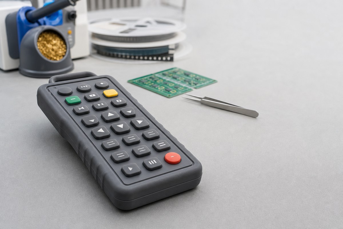
An industrial remote spends its life being pressed with a thumb, at whatever angle the operator happens to be holding it. That means the pill-to-pad interface is being loaded off-axis most of the time. A keypad with a perfectly centred pill and a shallow key wall can still read badly if the wall allows the key to cock sideways under an off-centre press.
Other Causes That Can Be Mistaken for Carbon Pill Distribution Problems
We have seen a full tool rebuilt for a problem that turned out to be flux residue. Before authorising a mould change, rule out these:
- PCB contamination, particularly no-clean flux that was never designed to be left on a contact pad
- Oxide or tarnish on the pad surface, which is common on boards that have sat in storage
- Pad geometry that is too narrow or too widely spaced for the pill diameter
- Insufficient key travel, so the pill never reaches full compression
- Excessive pre-load, which holds the pill permanently compressed and accelerates set
- Pill wear after a high number of actuations, visible as a polished or crazed contact face
- Keypad deformation caused by the housing, not by the keypad itself
- Assembly misalignment between the keypad, the spacer and the board
The practical discipline is to test the keypad standalone first, then the keypad on the board, then the finished unit. If the standalone spread is tight and the assembled spread is wide, the mould is not the problem.
How to Test Contact Resistance Across a Production Batch
Test Multiple Key Positions
Testing one representative button is worse than testing none, because it produces a number that looks authoritative. Sample the centre of the keypad, the edges, and at least two different cavities if the tool is multi-cavity.
Use the Same Compression Conditions
Contact resistance is a function of applied force and travel. If one measurement is taken with a thumb and the next with a spring probe at a different stroke, the two numbers are not comparable. Fix the force and record the travel.
Record a Distribution, Not a Pass or Fail
A single limit value hides the shape of the process. Record minimum, maximum, average, spread across positions, and spread between batches. A batch reading 120 to 160 ohms is healthier than one reading 80 to 380 ohms even if both have the same average.
Compare Samples Before and After Assembly
Standalone, on-board and finished-unit measurements should be taken on the same parts. The differences between them localise the cause far faster than any amount of argument.
Design Considerations for More Consistent Conductive Silicone Keypads
Consistency is cheaper to design in than to inspect out. The parameters that matter are the pill diameter relative to the pad pair, the finished pill thickness, the contact travel, the compression ratio at full actuation, the key wall thickness, the spacing between adjacent pills, the mould structure, and the PCB contact layout.
| Design parameter | What it controls | Typical failure if neglected |
|---|---|---|
| Pill diameter vs pad pair | Tolerance to lateral shift | Partial contact on offset keys |
| Finished pill thickness | Compression available before bottoming | Hard feel, or no reliable contact |
| Key wall thickness | Resistance to cocking under off-axis press | Angle-dependent readings |
| Contact travel | Compression window | Intermittent contact over life |
| Pill-to-pill spacing | Flow balance between cavities | Systematic position-to-position spread |
What a supplier can actually control
The controllable part of this problem sits in four places: mould dimensional control, consistency of the conductive compound, positional control of the pre-form, and a first-piece plus in-process inspection routine that measures the pill rather than only the keypad outline.
When a customer sends us a resistance spread to investigate, we start by measuring the pill on a set of samples from different cavities before touching the mould. More often than not the measurement decides the direction, and the mould stays as it is.
How a Silicone Keypad Manufacturer Can Control Conductive Contact Consistency
Useful supplier-side controls include mould dimensional inspection against the drawing, controlled preparation and storage of the conductive compound, documented pre-form positioning, recorded moulding parameters per batch, cure consistency, first-piece inspection on every run, resistance testing at defined force and travel, batch sampling rather than single-part testing, and dimensional inspection of the finished pill.
None of this is exotic. It is simply the difference between a supplier who can hand you the data and one who can only hand you the parts. Custom keypads with conductive pills are described on our custom silicone rubber keypad page, and the drawing questions we normally need answered are listed under technical support.
Troubleshooting Checklist for Uneven Contact Resistance
- Check conductive pill position against the intended centre
- Check pill dimensions, including flatness of the contact face
- Measure resistance at several positions, not one
- Check keypad compression and travel under a fixed force
- Inspect mould alignment and parting-line condition
- Review moulding temperature and cure parameters for the batch
- Inspect PCB contact surfaces for flux, oxide or mask
- Compare samples from different cavities
- Compare samples from different production batches
- Repeat the measurement after assembly to separate keypad from board
FAQ
What causes inconsistent resistance in a silicone keypad?
Most commonly it is a combination of pill geometry variation and contact-area variation rather than a single fault. Moulding consistency sets the pill, but compression, key wall stiffness and PCB surface condition decide how much of that pill actually touches copper.
Can molding pressure affect conductive pill resistance?
Yes. Closing pressure changes the flat area of the pill face and the local density of the carbon network, so it shifts the whole batch rather than one key. That is why pressure is recorded per run.
Why do some keypad buttons have higher resistance than others?
Look first at cavity position and pre-form placement, then at key wall thickness. A key that can cock slightly under an off-axis press will read differently from one that cannot, even with identical pills.
How should conductive silicone keypad resistance be tested?
At a fixed force and fixed travel, at multiple positions, with the result recorded as a distribution. Measure the keypad standalone, then on the board, then in the finished unit so the cause can be localised. The electrode and resistance measurement approach for antistatic and conductive rubber products is described in ISO 2878:2017.
Does conductive pill thickness affect contact resistance?
It affects the compression available before the key bottoms out, and therefore affects how quickly resistance rises once the pill is fully flattened. Thicker is not automatically better; the right value is the one that keeps the pill inside its compression window across the tolerance stack.
Can mold design improve conductive keypad consistency?
It can remove systematic error, which is often the largest single contribution. Balancing flow between cavities, controlling the parting line at the contact area and holding cavity dimensions tightly all reduce position-to-position spread.
FromRubber is a silicone and rubber keypad manufacturer in Dongguan, China, working with equipment and instrument builders on conductive keypad projects from drawing to production. If you are chasing a resistance spread and want a second measurement set, send the drawing, the PCB pad layout and the measured values to nani@fromrubber.com or karl@fromrubber.com. We also answer technical questions by WeChat and WhatsApp on +86 18676210913. For background on how we approach keypad design and moulding topics, see the silicone keypad technology articles.
Sources
- ISO 2878:2017, Rubber, vulcanized or thermoplastic — Antistatic and conductive products — Determination of electrical resistance. https://www.iso.org/standard/72778.html
- ISO 48-4:2018, Rubber, vulcanized or thermoplastic — Determination of hardness — Part 4: Indentation hardness by durometer method (Shore hardness). https://www.iso.org/standard/74969.html
- ISO 188:2023, Rubber, vulcanized or thermoplastic — Accelerated ageing and heat resistance tests. https://www.iso.org/standard/80468.html