Case Study: 22% Conductive Silicone Keypad Failure from Edge Thinning
You ship 8,000 handheld units. The silicone keypads pass every check. The factory inspector signs off. The customer's own quality team puts a green sticker on the shipment.
Ten days later, the calls start coming.
Not from everyone – just enough to set off alarms. The final number: 22% of those units came back. The symptom was always the same: some buttons worked fine in the factory but refused to respond after a few hours in warm, humid weather. In the lab, at a comfortable room temperature, the same buttons measured perfectly fine. The failure was intermittent – the worst kind to chase.
This happened to a product line we were asked to help salvage. What we found turned out to be hiding inside a single, innocent-looking number on the supplier's test report.
Conductive Silicone Keypad Failure: The Problem Shows Up
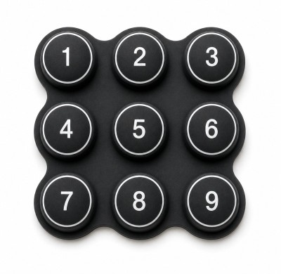
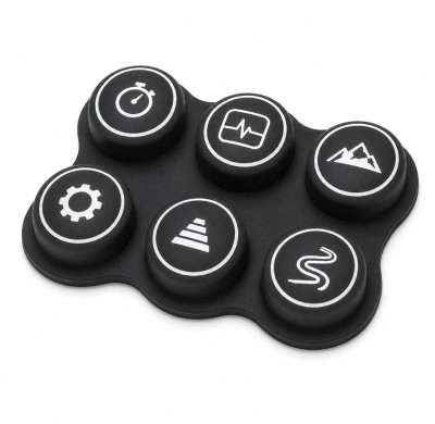
The product was a portable diagnostic tool used by field technicians outdoors. Its user interface relied on a 2×6 silicone rubber key mat – twelve dome-shaped keys molded as one soft sheet. Under each dome, there was a printed carbon pad. When you pressed a key, that carbon pad touched two exposed copper traces on the circuit board underneath, closing the circuit. The specification said the electrical path had to measure 90 ohms or less for the machine to register a keypress reliably.
The first batch was fine – fewer than 2 out of every 100 came back. Everyone was happy. Then they ramped up production, and the trouble began.
The returned units came with a very specific fingerprint:
- The two rightmost keys in the middle row – call them position #7 and #8 – accounted for most of the complaints.
- Those keys worked when tested in the service center, which was air-conditioned.
- But they failed in places like coastal Texas, Florida, and Southeast Asia – where the air is hot and sticky.
- In dry inland areas, almost none failed.
This pattern told us something important: humidity and heat were making a hidden weakness visible.
What We Found When We Dug Deeper into the Conductive Silicone Keypad
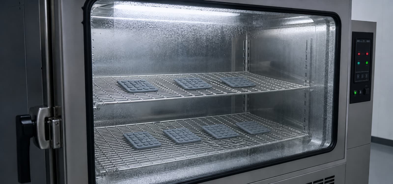
We took a batch of suspect keypads and put them into a temperature-and-humidity chamber – set to 80°C with 80% relative humidity. Then we measured those troublesome keys every few hours.
Here is what the meter showed:
| Soak Time (hours) | Contact Resistance – Key #8 | Observed Behaviour |
|---|---|---|
| 0 | 84 Ω | Pass |
| 3 | 142 Ω | Intermittent misses |
| 6 | 198 Ω | Frequent misses |
| 12 | 290 Ω | Consistent failure |
The same part that passed inspection was failing predictably under conditions that mimicked real-world outdoor use.
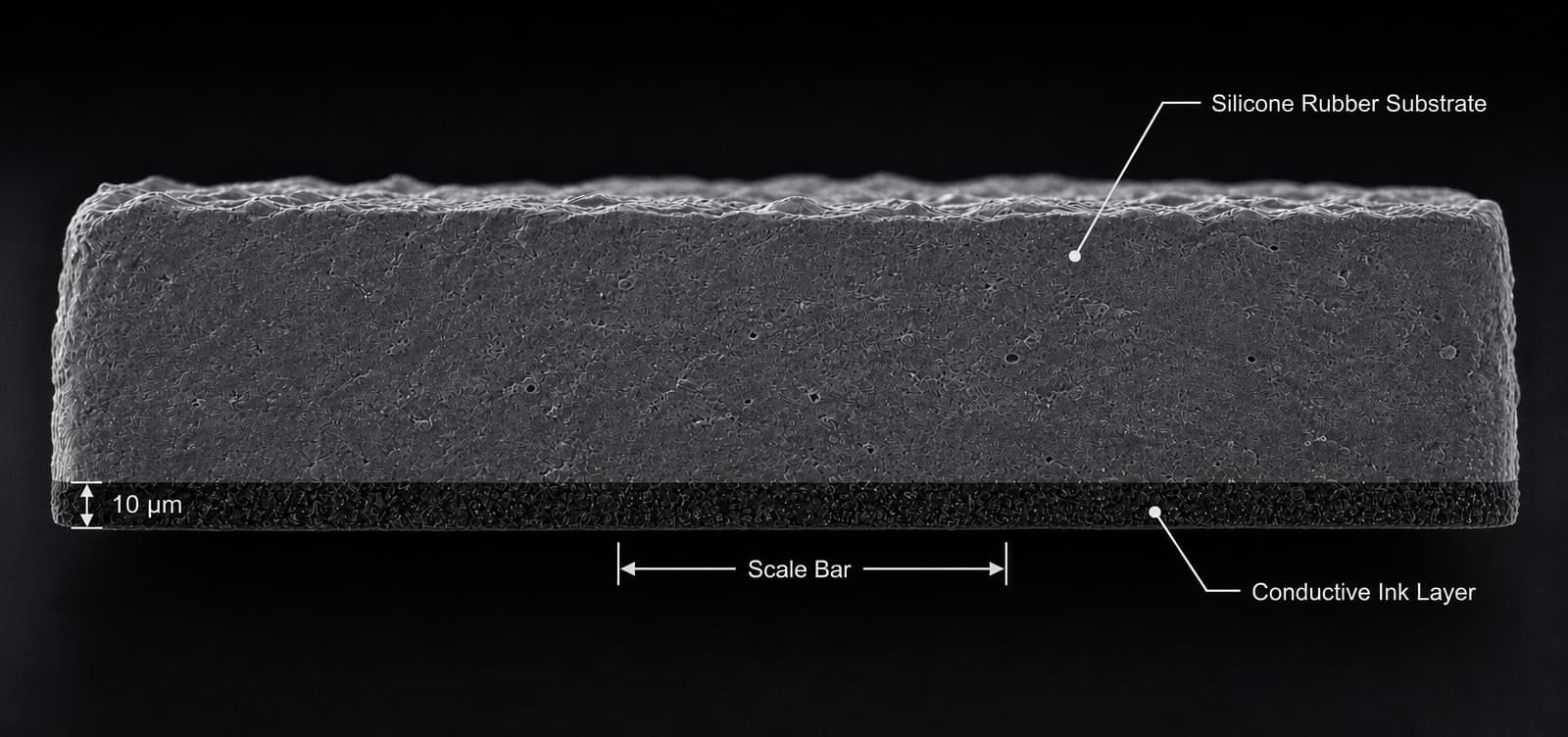
So we cut one of the failing keypads open to look at the carbon pad under a microscope. That is when we found the real issue.
The supplier's certificate said: "Average carbon ink thickness: 12 micrometres – specification: 10 to 14 – PASS."
But "average" was the problem. Imagine five students with an average height that looks fine – except one of them is severely undernourished. The average hides the weakest individual.
During screen printing – which works a bit like a stencil and a squeegee – the centre of the screen gets more ink because the squeegee presses hardest there. The edges get less, especially after the screen has been used a few hundred times. The screen stretches slightly, and the corners start to starve.
When we measured key position #8 – the bad one – the actual thickness was only 7.2 micrometres. Meanwhile, a key in the centre measured 13.8 micrometres. The average was 12, which looked great on paper. But that corner key was getting barely half the carbon it needed.
Here is the kicker: carbon ink thickness and electrical resistance are not friends in a straight line. Once you drop below about 9 micrometres, the resistance climbs very fast. At 7.2, it is already fragile. Add heat and moisture – which make the ink swell and the copper traces oxidize – and that fragile connection becomes an open circuit in just a few hours.
The math hurt: 1,760 returned units, roughly $72 each in shipping, repairs, and customer compensation. That is over $126,000 lost – not counting the angry customers and delayed projects – because one edge key was printed 5 micrometres too thin and nobody measured it separately.
How We Turned the Conductive Silicone Keypad Issue Around
We did not redesign the keypad. We did not change the plastic or the rubber compound. We fixed the measurement and control system around it. Here is what we did differently.
First, we stopped averaging. The new rule was simple: every key position gets its own minimum thickness. The centre keys needed at least 10.5 micrometres. The edge and corner keys – the ones that suffer from screen tension loss – needed at least 11.5 micrometres. We set the bar higher for the edges, not lower.
Second, we changed how we measure. The old way used a laser profilometer, which scans the surface from above. But silicone rubber has a textured surface, and the instrument reads the texture plus the ink together – overreporting thickness by 2 or 3 micrometres. It was giving false confidence. We switched to cross-sectioning: cutting a key out, polishing the cut edge, and measuring it under a microscope at 100x magnification. It destroys one keypad per test, but it gives you the real number, not an estimate.
Third, we started watching the screen tension during printing. The printing screen is like a fine mesh stretched on a frame. After about 350 to 400 strokes, the tension drops and the edges print thinner. Instead of waiting for defects to appear – which was too late – the operator began checking tension every 50 strokes and replacing the screen proactively. This kept the edge keys healthy throughout the whole run.
Fourth, we added a baking step after curing. The printed carbon ink contains solvents that need to fully evaporate and cross-link. A 3-hour bake at 150°C drove out the leftovers and made the ink layer denser – less porous, so moisture could not creep in as easily.
Fifth, we recommended a small change to the circuit board. The original used bare copper pads with a thin organic coating. Copper oxidises over time, especially in humidity, and that oxide layer adds resistance. We switched to ENIG – electroless nickel immersion gold – a standard finish in many electronics. It costs about 3 cents more per keypad, but it completely removes the oxidation variable.
With these five changes, the next production run came back with a failure rate of just over 2% – and most of those were traced to unrelated assembly problems, not the keypad.
Five Lessons for Conductive Silicone Keypad Reliability
If you take nothing else from this story, remember these five points. They are not theory – they are scars from real work.
- 1. The average is a liar.
When you have multiple points in a system – like 12 keys on one mat – the average tells you nothing about the weakest one. And in electronics, the weakest one decides whether the whole device works. Always check the corners. Always check the edges. They are where the process breaks down first. - 2. Test under real-world conditions before shipping.
If we had only relied on room-temperature measurements, we would have never found the problem. Humidity and heat are not optional extras – they are part of the real environment. A simple 200-hour damp-heat test would have caught this issue before the first batch went out the door. - 3. Copper is not your friend in a wet environment.
Bare copper oxidises. It is a fact of chemistry. If your carbon pad touches bare copper, that contact resistance will drift upward over time. Use gold-plated pads (ENIG or hard gold). It is a tiny cost for a massive reliability boost. - 4. Measure the whole assembly, not just the loose part.
A carbon pad might read fine on a test fixture, but when it is mounted, compressed, and screwed into a housing, the numbers change. Alignment, warpage, and how the dome collapses all affect contact. Always test fully built units with the actual force a user would apply. - 5. Watch the process, not just the result.
Incoming inspection only catches problems after they have happened. The real control is on the production floor – screen tension, squeegee speed, ink viscosity, and how often you change the screen. If you only look at the final part, you are always reacting. If you watch the process, you can prevent.
A Side Note on How We Engineer Conductive Silicone Keypads
At FromRubber, we see stories like this not as warnings – but as blueprints. Every time we help a customer with a custom silicone keypad for home appliances, medical devices, or industrial tools, we bring this exact thinking to the table.
We do not guess. We cut, measure, and test by position. We share raw data, not just pass/fail checkmarks. We ask about your environment – dry desert, humid coast, or something in between – and we match the carbon formulation and PCB finish to that reality.
We have been molding silicone keypads since 2011. We do not use fancy slogans. We use microscopes, environmental chambers, and field-return analysis. If you are working on a silicone keypad project and want to avoid the "average thickness" trap, we would be happy to take a look at your drawing and test plan – no charge, just engineering.